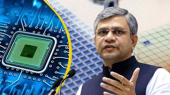
New Delhi: Union Minister for Electronics and Information Technology, Railways, and Information & Broadcasting, Ashwini Vaishnaw has shared a video explaining how the chips used in everyday products are made, taking viewers through the journey from silica sand to finished semiconductor devices.
The video shows how silica sand is converted into silicon ingots, sliced into wafers and then put through fabrication, assembly, testing and packaging. These tiny chips eventually find applications in products ranging from phones and cars to trains. The simple visual explanation comes as India is expanding its semiconductor manufacturing and design capabilities.
The chip journey, simplified. pic.twitter.com/dZIqkX5QvR
— Ashwini Vaishnaw (@AshwiniVaishnaw) August 31, 2026
The push is gaining momentum with the government’s Semicon 2.0 programme, which has an outlay of ₹1.27 lakh crore and provides support of up to 40% for semiconductor fabs. At the state level, Tamil Nadu has also announced a ₹175 crore Semiconductor and Electronics Manufacturing Park in Kancheepuram, expected to attract around ₹2,000 crore in investments and create about 5,000 jobs.
Vaishnaw’s video offers a quick look at the complex process behind one of the most important technologies in modern life, while highlighting the larger ambition of building India’s semiconductor ecosystem around “Build in Bharat. Design in Bharat.”
BI Bureau